South Korea Semiconductor Production Equipment Market Report: Trends, Growth and Forecast (2026-2032)
By Equipment Type (Wafer Fabrication Equipment (Lithography Equipment, Etching Equipment, Deposition & Epitaxy Equipment, Metrology, Inspection & Process Control Equipment, Others), Assembly & Packaging Equipment (Dicing & Singulation Equipment, Die Bonding Equipment, Wire Bonding & Flip-Chip Bonding Equipment, Molding, Encapsulation & Advanced Packaging Equipment, Others), Semiconductor Test Equipment (Wafer Probing Equipment, Automated Test Equipment, Burn-in & Reliability Test Equipment, Final Test & System-Level Test Equipment, Others)), By Wafer Size (300 mm, 200 mm, 150 mm, Others), By Technology Node (Leading-Edge Nodes (≤5 nm), Advanced Nodes (>5 nm to 14 nm), Mature Nodes (>14 nm to 90 nm), Legacy Nodes (>90 nm), Others), By Semiconductor Device Type (Logic & Micro component Devices, Memory Devices, Analog & Mixed-Signal ICs, Discrete, Power & Optoelectronic Devices, MEMS & Sensor Devices, Others), By End User (Foundries, Integrated Device Manufacturers, OSAT Companies, Research Institutes & Universities, Others), By Region (North, East, West, South) ... Read more
|
Major Players
|
South Korea Semiconductor Production Equipment Market Overview
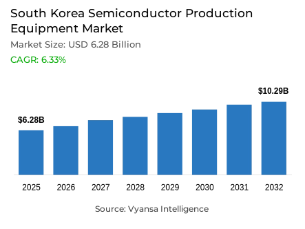
Semiconductor production equipment comprises the machinery and systems used for wafer fabrication, lithography, deposition, etching, packaging, inspection, metrology, testing, and process control throughout semiconductor manufacturing. The South Korea semiconductor production equipment market is projected to grow at a CAGR of 6.33% during 2026–2032, driven by expanding memory, foundry, and advanced packaging capacity.
Key Highlights of the South Korea Semiconductor Production Equipment Market
- South Korea semiconductor production equipment market stood at USD 6.28 billion in 2025 and reached USD 7.12 billion in 2026, with value expected to reach USD 10.29 billion by 2032.
- The market is forecast to grow at a CAGR of 6.33% during 2026-2032.
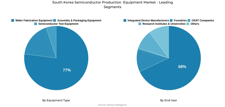
- Based on equipment type, Wafer Fabrication Equipment leads the industry with 77% share in 2026.
- However, semiconductor test equipment is the fastest-growing equipment type, expanding at a CAGR of 11% during 2026-2032.
- By end user, Integrated Device Manufacturers lead the industry with 68% share in 2026.
- Meanwhile, Foundries are the fastest-growing end-user category, expanding at a CAGR of 18% during 2026-2032.
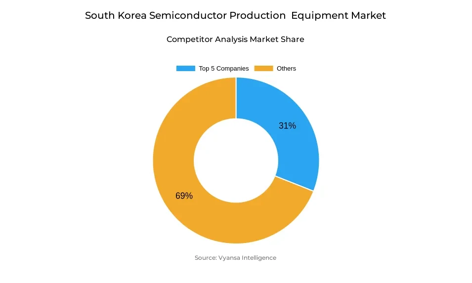
- The top five companies account for 31% of the market, indicating moderate consolidation across lithography, etching, deposition, metrology, inspection, packaging, and semiconductor test equipment segments.
The semiconductor production equipment market in South Korea is gaining commercial significance because Korean semiconductor manufacturers need high-precision tools to convert wafers into qualified memory semiconductors, logic devices, foundry chips, and packaged components. Lithography equipment, etching equipment, deposition equipment, cleaning equipment, metrology equipment, inspection equipment, and process control equipment directly influence wafer throughput, defect reduction, yield optimization, die cost, and customer qualification.
Additionally, the demand is concentrated among integrated device manufacturers, while foundries, OSAT companies, packaging houses, research institutes, and universities widen the addressable base. Wafer fabrication equipment dominates because front-end equipment defines pattern accuracy, film quality, process repeatability, memory nodes, logic nodes, and high-volume wafer processing efficiency. However, back-end equipment demand is strengthening as HBM, advanced DRAM, AI chips, and system-level devices require bonding accuracy, thermal reliability, wafer probing equipment, automated test equipment, and final test equipment.
Policy and infrastructure support are strengthening the South Korea semiconductor equipment market. The Ministry of Science and ICT stated that the mega cluster covers Pyeongtaek, Hwaseong, Yongin, Icheon, Anseong, Pangyo, and Suwon, creating a dense semiconductor cluster for fab capacity expansion, process engineering, supplier co-location, tool qualification, spare parts, and local maintenance services.
Over the forecast period, semiconductor production equipment companies in South Korea are expected to compete through local engineering capability, spare-parts availability, compliance documentation, equipment uptime, process-development support, and direct integration with Korean semiconductor fabs. Competitive success will depend on supporting memory fab upgrades, advanced node investment, HBM packaging, foundry expansion, back-end automation, and high-volume wafer processing.
Korea’s Semiconductor Policy and Equipment Compliance Framework Supporting Tool Adoption
South Korea’s semiconductor production equipment market operates within a strategic policy environment shaped by semiconductor cluster planning, high-tech industry protection, export-control governance, and fab infrastructure development. The semiconductor mega-cluster plan supports expansion across the Gyeonggi-do fab cluster through existing fabs, planned fabs, and private investment. This strengthens demand for 300 mm wafer equipment, high-volume wafer processing tools, inspection equipment, process control equipment, and cleanroom-ready installation services.
The National High-Tech Strategic Industry framework requires approval when a holder intends to export national high-tech strategic technology, which affects sensitive process know-how, equipment technology transfer, and cross-border cooperation. For suppliers, this increases the importance of documentation, local compliance teams, secure software access, authorized field service, controlled technical support, and verified tool-qualification systems. Companies with local engineering strength, export-control discipline, and strong customer support capabilities are better positioned to secure long-term relationships with Korean semiconductor fabs.
South Korea Semiconductor Production Equipment Market Drivers
HBM-Led Capacity Upgrades and Advanced Node Investment
The primary driver is the expansion of HBM, DRAM production, NAND flash production, and advanced node investment, which increases demand for wafer fabrication equipment, lithography equipment, etching equipment, deposition equipment, cleaning equipment, metrology equipment, inspection equipment, and process control equipment. Korean memory manufacturers require tighter process windows to improve stack density, bandwidth, yield, and thermal reliability. This creates recurring demand because every technology transition requires new tools, validated recipes, maintenance support, and spare-parts planning before volume production stabilizes.
SEMI’s 2026 equipment-billings release shows how memory chip production converts into equipment demand. Korea’s semiconductor equipment spending reached USD 25.8 billion in 2025, increasing 26% year-on-year, while worldwide equipment billings reached USD 135.1 billion. This Korea-specific growth indicates active fab capacity expansion, and the demand link is direct because higher wafer starts, advanced memory output, and HBM packaging require front-end equipment, inspection systems, semiconductor test equipment, and back-end equipment.
Restraints
High Equipment Cost, Export-Control Risk, and Long Qualification Cycles
One of the key restraints in the South Korea semiconductor equipment market is dependence on high-cost, imported, and technology-intensive production tools. Lithography equipment, metrology equipment, etching equipment, deposition equipment, and 300 mm wafer equipment require restricted components, controlled software access, cleanroom installation, skilled field engineers, and fab-specific calibration. These requirements increase maintenance costs, raise installation complexity, and make yield optimization difficult when equipment delivery lead times, calibration delays, or limited vendor support affect production ramp-up.
The restraint is further intensified by export-control risk and compliance obligations. The U.S. Bureau of Industry and Security stated in February 2026 that Applied Materials Inc. and Applied Materials Korea, Ltd. agreed to pay approximately USD 252 million to settle allegations involving illegal exports of U.S. semiconductor manufacturing equipment to China. This raises the commercial burden of export-license screening, end-use checks, spare-parts release, controlled software access, and re-export governance for multinational suppliers operating through Korean subsidiaries or assembly routes.
Recent Trends
Advanced Packaging Equipment and Back-End Automation
Advanced packaging equipment and back-end automation are moving from supporting functions into central growth areas for semiconductor production equipment in South Korea. HBM devices, advanced memory devices, and AI chips require tighter bonding, wafer probing equipment, automated test equipment, burn-in test equipment, reliability test equipment, and system-level test equipment before shipment. This differs from earlier capacity expansion cycles because Korean fabs and OSAT companies now need back-end equipment that supports traceability, throughput, dense package architectures, and shipment-quality documentation.
Companies are responding by expanding Korea-based application engineering, R&D, and service footprints. ASML supports Korean semiconductor manufacturers with lithography systems and technical services, while Lam Research opened its Korea Technology Centre to support semiconductor equipment and process technology development. Tokyo Electron Korea also provides service, sales support, and R&D for semiconductor production equipment in Korea. These investments strengthen customer-proximate qualification, process support, and long-term field-service capability for advanced semiconductor manufacturing.
Metrology, Inspection, and Atomic-Scale Process Control
The technical trend is the shift toward metrology equipment, inspection equipment, process control equipment, AI-based inspection, smart fab equipment, and advanced process monitoring. Advanced nodes, memory nodes, logic nodes, DRAM process equipment, and NAND flash process equipment require thinner films, tighter critical-dimension control, precise material removal, defect detection, and faster yield learning. This makes equipment differentiation move beyond throughput toward process repeatability, defect reduction, reliability, and high-volume wafer fabrication performance.
Applied Materials states that its semiconductor equipment can deposit layers on wafers, shape and remove materials with atomic precision, analyze materials, and integrate devices. SEMES also states that it is Korea’s largest equipment manufacturer, producing key semiconductor and display equipment worth approximately KRW 3 trillion annually. Its portfolio covers cleaning equipment, etching equipment, photo-track systems, probing equipment, bonding equipment, and test handlers, supporting domestic capability across front-end and back-end production workflows.
Future Opportunities
Memory Fab Upgrades, Foundry Expansion, and HBM Packaging Equipment
Memory fab upgrades, foundry capacity expansion, advanced packaging demand, and semiconductor test equipment demand represent the strongest opportunity areas. Korean manufacturers expanding high-bandwidth memory production and advanced memory devices require integrated front-end and back-end workflows. Existing wafer fabrication equipment strength does not remove back-end bottlenecks because HBM packaging equipment must support bonding accuracy, die traceability, thermal control, wafer-level packaging, chip testing services, and reliability screening.
The opportunity is supported by Korea’s 2026 AI-chip investment push. According to the recent report, the South Korea announced major chip and AI mega projects involving Samsung Electronics and SK Hynix, including new fabrication facilities, HBM-related capacity, and a large chip-packaging cluster in Chungcheong. This supports monetization for equipment suppliers through local application labs, field-service teams, certified installation, co-development, semiconductor supply chain resilience, and long-term maintenance contracts.
Unlock Market Intelligence
Explore the market potential with our data-driven report
South Korea Semiconductor Production Equipment Market Segmentation Analysis
By Equipment Type
- Wafer Fabrication Equipment
- Lithography Equipment
- Etching Equipment
- Deposition & Epitaxy Equipment
- Metrology, Inspection & Process Control Equipment
- Others
- Assembly & Packaging Equipment
- Dicing & Singulation Equipment
- Die Bonding Equipment
- Wire Bonding & Flip-Chip Bonding Equipment
- Molding, Encapsulation & Advanced Packaging Equipment
- Others
- Semiconductor Test Equipment
- Wafer Probing Equipment
- Automated Test Equipment
- Burn-in & Reliability Test Equipment
- Final Test & System-Level Test Equipment
- Others
Wafer Fabrication Equipment Leads, While Semiconductor Test Equipment Expands Faster
Wafer Fabrication Equipment leads the equipment type segment with 77% share in 2026 because South Korea’s production base is anchored in front-end equipment for memory nodes, logic nodes, and high-volume wafer processing. Lithography equipment, etching equipment, deposition equipment, epitaxy equipment, cleaning equipment, metrology equipment, inspection equipment, and process control equipment carry high value and directly affect yield, wafer throughput, defect reduction, and customer qualification.
Meanwhile, Semiconductor Test Equipment is the fastest-growing equipment type, expanding at a CAGR of 11% during 2026-2032. Growth is supported by HBM devices, advanced memory devices, DRAM, NAND flash, AI chips, and system semiconductors that require wafer probing equipment, automated test equipment, burn-in test equipment, reliability test equipment, final test equipment, and system-level test equipment. Compared with wafer fabrication equipment, test equipment grows faster because stacked packages and AI memory shipments require deeper validation before customer delivery.
By End User
- Foundries
- Integrated Device Manufacturers
- OSAT Companies
- Research Institutes & Universities
- Others
Integrated Device Manufacturers Lead, While Foundries Accelerate Growth
Integrated Device Manufacturers lead the end-user segment with 68% share in 2026 because Samsung Electronics and SK hynix operate large domestic semiconductor fabs, memory manufacturing bases, and high-volume wafer fabrication ecosystems. Their scale supports recurring procurement of lithography equipment, deposition equipment, etching equipment, inspection equipment, metrology equipment, bonding systems, and semiconductor test equipment. IDMs lead because they control wafer starts, DRAM production, NAND flash production, HBM capacity planning, and supplier qualification.
Meanwhile, Foundries are the fastest-growing end-user category, expanding at a CAGR of 18% during 2026-2032. Growth is linked to foundry expansion, logic chip production, system semiconductors, AI chips, and advanced node semiconductor production. Foundries require foundry process equipment for customer-specific qualification, yield learning, metrology, inspection, and fab capacity expansion. Compared with IDMs, foundries start from a smaller equipment base, so new fab modules and customer tape-outs generate faster incremental equipment demand.
Unlock Market Intelligence
Explore the market potential with our data-driven report
South Korea Semiconductor Production Equipment Market Regional Analysis
Gyeonggi-do Leads Through the Core Semiconductor Mega Cluster
Gyeonggi-do is the leading sub-regional cluster in South Korea semiconductor manufacturing equipment market because it contains the Pyeongtaek semiconductor hub, Icheon memory production, Hwaseong, Yongin, Anseong, Pangyo, and Suwon within South Korea’s main semiconductor production corridor. The Ministry of Science and ICT stated that the mega cluster currently features 19 production fabs and two R&D fabs, with 16 new fabs planned by 2047. This Gyeonggi-do fab cluster supports lithography service, etch and deposition support, inspection equipment, spare parts, local application engineering, and tool qualification.
Key Companies in the South Korea Semiconductor Production Equipment Market
- ASML Korea Co., Ltd.
- Applied Materials Korea, Ltd.
- Lam Research Manufacturing Korea LLC / Lam Research Korea
- Tokyo Electron Korea Ltd.
- SEMES Co., Ltd.
- KLA Korea
- Wonik IPS Co., Ltd.
- ASM Korea Ltd.
- Advantest Korea Co., Ltd.
- Hanmi Semiconductor Co., Ltd.
Company Profiling
The profiles below assess equipment relevance, technical capability, Korean operating presence, customer proximity, manufacturing or service support, and competitive role in semiconductor production.
ASML Korea Co., Ltd.
ASML Korea Co., Ltd. is the Korean operating presence of ASML, the Netherlands-based lithography equipment company. Its market connection is advanced lithography equipment used in front-end semiconductor equipment workflows for high-volume wafer processing and advanced node investment. SK hynix’s 2026 plan to purchase 11.95 trillion won of ASML EUV lithography tools by December 2027 shows ASML’s relevance to Korean HBM, DRAM, and advanced memory production. ASML Korea is positioned as a technology-led lithography supplier for leading-edge nodes.
Applied Materials Korea, Ltd.
Applied Materials Korea, Ltd. is the Korean subsidiary of Applied Materials, Inc., a U.S.-headquartered semiconductor equipment supplier. Its relevant portfolio includes deposition equipment, etching-related process systems, materials engineering tools, process control equipment, and wafer fabrication equipment used to deposit, remove, modify, analyze, and connect materials. These systems support Korean IDMs and foundries across DRAM, NAND flash, logic devices, and foundry chips. The company is positioned as a portfolio-led process equipment supplier serving advanced semiconductor manufacturing.
Lam Research Manufacturing Korea LLC / Lam Research Korea
Lam Research Manufacturing Korea LLC / Lam Research Korea participates through front-end equipment used in etching, deposition, strip, clean, and advanced process applications. Lam’s Korea Technology Center supports semiconductor equipment and process technology development, strengthening customer-proximate engagement with Korean semiconductor fabs. Its equipment capability is relevant to memory manufacturers, foundries, high-volume wafer fabrication, and advanced process monitoring where plasma control, film precision, and repeatability matter. Lam is positioned as a customer-proximate process-technology participant.
Tokyo Electron Korea Ltd.
Tokyo Electron Korea Ltd. is a Korean group company of Tokyo Electron Limited, with its head office in Hwaseong, Gyeonggi-do. The company provides service, sales support, and R&D for semiconductor production equipment in Korea. Its broader portfolio supports coater and developer systems, etching equipment, deposition equipment, cleaning equipment, thermal processing, wafer bonding, and wafer probing equipment. Tokyo Electron Korea is positioned as a process-integration and service-support participant for Korean fabs.
SEMES Co., Ltd.
SEMES Co., Ltd. is a Korea-based semiconductor and display equipment manufacturer. SEMES describes itself as Korea’s largest equipment maker and identifies cleaning equipment, etching equipment, photo-track systems, bonding equipment, probing equipment, and test-handler equipment in its semiconductor portfolio. These products support both wafer fabrication equipment and back-end equipment requirements for Korean semiconductor production lines. SEMES is positioned as a domestic manufacturing specialist with localization strength, broad equipment coverage, and relevance to Korean semiconductor supply chain resilience.
Recent Developments and Updates
- March 2026: SK hynix announced plans to procure KRW 11.95 trillion worth of EUV lithography equipment from ASML by December 2027, marking the company's largest publicly disclosed equipment order. The investment will support next-generation memory chip production, including HBM and advanced DRAM, as well as capacity expansion at its Yongin and Cheongju manufacturing facilities. This development is expected to significantly strengthen demand for leading-edge lithography equipment across South Korea's semiconductor manufacturing ecosystem.
Frequently Asked Questions
Related Report
- Market Segmentation
- Research Scope
- Research Methodology
- Definitions and Assumptions
- Executive Summary
- South Korea Semiconductor Production Equipment Market Policies, Regulations, and Standards
- South Korea Semiconductor Production Equipment Market Dynamics
- Growth Factors
- Challenges
- Trends
- Opportunities
- South Korea Semiconductor Production Equipment Market Statistics, 2022-2032F
- Market Size & Growth Outlook
- By Revenues in USD Million
- Market Segmentation & Growth Outlook
- By Equipment Type
- Wafer Fabrication Equipment- Market Insights and Forecast 2022-2032, USD Million
- Lithography Equipment- Market Insights and Forecast 2022-2032, USD Million
- Etching Equipment- Market Insights and Forecast 2022-2032, USD Million
- Deposition & Epitaxy Equipment- Market Insights and Forecast 2022-2032, USD Million
- Metrology, Inspection & Process Control Equipment- Market Insights and Forecast 2022-2032, USD Million
- Others- Market Insights and Forecast 2022-2032, USD Million
- Assembly & Packaging Equipment- Market Insights and Forecast 2022-2032, USD Million
- Dicing & Singulation Equipment- Market Insights and Forecast 2022-2032, USD Million
- Die Bonding Equipment- Market Insights and Forecast 2022-2032, USD Million
- Wire Bonding & Flip-Chip Bonding Equipment- Market Insights and Forecast 2022-2032, USD Million
- Molding, Encapsulation & Advanced Packaging Equipment- Market Insights and Forecast 2022-2032, USD Million
- Others- Market Insights and Forecast 2022-2032, USD Million
- Semiconductor Test Equipment- Market Insights and Forecast 2022-2032, USD Million
- Wafer Probing Equipment- Market Insights and Forecast 2022-2032, USD Million
- Automated Test Equipment- Market Insights and Forecast 2022-2032, USD Million
- Burn-in & Reliability Test Equipment- Market Insights and Forecast 2022-2032, USD Million
- Final Test & System-Level Test Equipment- Market Insights and Forecast 2022-2032, USD Million
- Others- Market Insights and Forecast 2022-2032, USD Million
- Wafer Fabrication Equipment- Market Insights and Forecast 2022-2032, USD Million
- By Wafer Size
- 300 mm- Market Insights and Forecast 2022-2032, USD Million
- 200 mm- Market Insights and Forecast 2022-2032, USD Million
- 150 mm- Market Insights and Forecast 2022-2032, USD Million
- Others- Market Insights and Forecast 2022-2032, USD Million
- By Technology Node
- Leading-Edge Nodes (≤5 nm)- Market Insights and Forecast 2022-2032, USD Million
- Advanced Nodes (>5 nm to 14 nm)- Market Insights and Forecast 2022-2032, USD Million
- Mature Nodes (>14 nm to 90 nm)- Market Insights and Forecast 2022-2032, USD Million
- Legacy Nodes (>90 nm)- Market Insights and Forecast 2022-2032, USD Million
- Others- Market Insights and Forecast 2022-2032, USD Million
- By Semiconductor Device Type
- Logic & Micro component Devices- Market Insights and Forecast 2022-2032, USD Million
- Memory Devices- Market Insights and Forecast 2022-2032, USD Million
- Analog & Mixed-Signal ICs- Market Insights and Forecast 2022-2032, USD Million
- Discrete, Power & Optoelectronic Devices- Market Insights and Forecast 2022-2032, USD Million
- MEMS & Sensor Devices- Market Insights and Forecast 2022-2032, USD Million
- Others- Market Insights and Forecast 2022-2032, USD Million
- By End User
- Foundries- Market Insights and Forecast 2022-2032, USD Million
- Integrated Device Manufacturers- Market Insights and Forecast 2022-2032, USD Million
- OSAT Companies- Market Insights and Forecast 2022-2032, USD Million
- Research Institutes & Universities- Market Insights and Forecast 2022-2032, USD Million
- Others- Market Insights and Forecast 2022-2032, USD Million
- By Region
- North- Market Insights and Forecast 2022-2032, USD Million
- East- Market Insights and Forecast 2022-2032, USD Million
- West- Market Insights and Forecast 2022-2032, USD Million
- South- Market Insights and Forecast 2022-2032, USD Million
- By Competitors
- Competition Characteristics
- Market Share & Analysis
- By Equipment Type
- Market Size & Growth Outlook
- South Korea Wafer Fabrication Equipment Market Statistics, 2022-2032
- Market Size & Growth Outlook
- By Revenues in USD Million
- Market Segmentation & Growth Outlook
- By Wafer Size- Market Insights and Forecast 2022-2032, USD Million
- By Technology Node- Market Insights and Forecast 2022-2032, USD Million
- By Semiconductor Device Type- Market Insights and Forecast 2022-2032, USD Million
- By End User- Market Insights and Forecast 2022-2032, USD Million
- By Region- Market Insights and Forecast 2022-2032, USD Million
- Market Size & Growth Outlook
- South Korea Lithography Equipment Market Statistics, 2022-2032
- Market Size & Growth Outlook
- By Revenues in USD Million
- Market Segmentation & Growth Outlook
- By Wafer Size- Market Insights and Forecast 2022-2032, USD Million
- By Technology Node- Market Insights and Forecast 2022-2032, USD Million
- By Semiconductor Device Type- Market Insights and Forecast 2022-2032, USD Million
- By End User- Market Insights and Forecast 2022-2032, USD Million
- By Region- Market Insights and Forecast 2022-2032, USD Million
- Market Size & Growth Outlook
- South Korea Etching Equipment Market Statistics, 2022-2032
- Market Size & Growth Outlook
- By Revenues in USD Million
- Market Segmentation & Growth Outlook
- By Wafer Size- Market Insights and Forecast 2022-2032, USD Million
- By Technology Node- Market Insights and Forecast 2022-2032, USD Million
- By Semiconductor Device Type- Market Insights and Forecast 2022-2032, USD Million
- By End User- Market Insights and Forecast 2022-2032, USD Million
- By Region- Market Insights and Forecast 2022-2032, USD Million
- Market Size & Growth Outlook
- South Korea Deposition & Epitaxy Equipment Market Statistics, 2022-2032
- Market Size & Growth Outlook
- By Revenues in USD Million
- Market Segmentation & Growth Outlook
- By Wafer Size- Market Insights and Forecast 2022-2032, USD Million
- By Technology Node- Market Insights and Forecast 2022-2032, USD Million
- By Semiconductor Device Type- Market Insights and Forecast 2022-2032, USD Million
- By End User- Market Insights and Forecast 2022-2032, USD Million
- By Region- Market Insights and Forecast 2022-2032, USD Million
- Market Size & Growth Outlook
- South Korea Metrology, Inspection & Process Control Equipment Market Statistics, 2022-2032
- Market Size & Growth Outlook
- By Revenues in USD Million
- Market Segmentation & Growth Outlook
- By Wafer Size- Market Insights and Forecast 2022-2032, USD Million
- By Technology Node- Market Insights and Forecast 2022-2032, USD Million
- By Semiconductor Device Type- Market Insights and Forecast 2022-2032, USD Million
- By End User- Market Insights and Forecast 2022-2032, USD Million
- By Region- Market Insights and Forecast 2022-2032, USD Million
- Market Size & Growth Outlook
- Competitive Outlook
- Company Profiles
- ASML Korea Co., Ltd.
- Business Description
- Product Portfolio
- Collaborations & Alliances
- Recent Developments
- Financial Details
- Others
- Applied Materials Korea, Ltd.
- Business Description
- Product Portfolio
- Collaborations & Alliances
- Recent Developments
- Financial Details
- Others
- Lam Research Manufacturing Korea LLC/ Lam Research Korea
- Business Description
- Product Portfolio
- Collaborations & Alliances
- Recent Developments
- Financial Details
- Others
- Tokyo Electron Korea Ltd.
- Business Description
- Product Portfolio
- Collaborations & Alliances
- Recent Developments
- Financial Details
- Others
- SEMES Co., Ltd.
- Business Description
- Product Portfolio
- Collaborations & Alliances
- Recent Developments
- Financial Details
- Others
- KLA Korea
- Business Description
- Product Portfolio
- Collaborations & Alliances
- Recent Developments
- Financial Details
- Others
- Wonik IPS Co., Ltd.
- Business Description
- Product Portfolio
- Collaborations & Alliances
- Recent Developments
- Financial Details
- Others
- ASM Korea Ltd.
- Business Description
- Product Portfolio
- Collaborations & Alliances
- Recent Developments
- Financial Details
- Others
- Advantest Korea Co., Ltd.
- Business Description
- Product Portfolio
- Collaborations & Alliances
- Recent Developments
- Financial Details
- Others
- Hanmi Semiconductor Co., Ltd.
- Business Description
- Product Portfolio
- Collaborations & Alliances
- Recent Developments
- Financial Details
- Others
- ASML Korea Co., Ltd.
- Company Profiles
- Disclaimer
| Segment | Sub-Segment |
|---|---|
| By Equipment Type |
|
| By Wafer Size |
|
| By Technology Node |
|
| By Semiconductor Device Type |
|
| By End User |
|
| By Region |
|
Research Methodology
This study followed a structured approach comprising four key phases to assess the size and scope of the electro-oxidation market. The process began with thorough secondary research to collect data on the target market, related markets, and broader industry context. These findings, along with preliminary assumptions and estimates, were then validated through extensive primary research involving industry experts from across the value chain. To calculate the overall market size, both top-down and bottom-up methodologies were employed. Finally, market segmentation and data triangulation techniques were applied to refine and validate segment-level estimations.
Secondary Research
The secondary research phase involved gathering data from a wide range of credible and published sources. This step helped in identifying industry trends, defining market segmentation, and understanding the market landscape and value chain.
Sources consulted during this phase included:
- Company annual reports, investor presentations, and press releases
- Industry white papers and certified publications
- Trade directories and market-recognized databases
- Articles from authoritative authors and reputable journals
- Gold and silver standard websites
Secondary research was critical in mapping out the industry's value chain and monetary flow, identifying key market segments, understanding regional variations, and tracking significant industry developments.
Other key sources:
- Financial disclosures
- Industry associations and trade bodies
- News outlets and business magazines
- Academic journals and research studies
- Paid industry databases
Primary Research
To validate secondary data and gain deeper market insights, primary research was conducted with key stakeholders across both the supply and demand sides of the market.
On the demand side, participants included decision-makers and influencers from end-user industries—such as CIOs, CTOs, and CSOs—who provided first-hand perspectives on market needs, product usage, and future expectations.
On the supply side, interviews were conducted with manufacturers, industry associations, and institutional participants to gather insights into current offerings, product pipelines, and market challenges.
Primary interviews provided critical inputs such as:
- Market size and revenue data
- Product and service breakdowns
- Market forecasts
- Regional and application-specific trends
Stakeholders consulted included:
- Leading OEM and solution providers
- Channel and distribution partners
- End users across various applications
- Independent consultants and industry specialists
Market Size Estimation and Data Triangulation
- Identifying Key Market Participants (Secondary Research)
- Goal: To identify the major players or companies in the target market. This typically involves using publicly available data sources such as industry reports, market research publications, and financial statements of companies.
- Tools: Reports from firms like Gartner, Forrester, Euromonitor, Statista, IBISWorld, and others. Public financial statements, news articles, and press releases from top market players.
- Extracting Earnings of Key Market Participants
- Goal: To estimate the earnings generated from the product or service being analyzed. This step helps in understanding the revenue potential of each market player in a specific geography.
- Methods: Earnings data can be gathered from:
- Publicly available financial reports (for listed companies).
- Interviews and primary data sources from professionals, such as Directors, VPs, SVPs, etc. This is especially useful for understanding more nuanced, internal data that isn't publicly disclosed.
- Annual reports and investor presentations of key players.
- Data Collation and Development of a Relevant Data Model
- Goal: To collate inputs from both primary and secondary sources into a structured, data-driven model for market estimation. This model will incorporate key market KPIs and any independent variables relevant to the market.
- Key KPIs: These could include:
- Market size, growth rate, and demand drivers.
- Industry-specific metrics like market share, average revenue per customer (ARPC), or average deal size.
- External variables, such as economic growth rates, inflation rates, or commodity prices, that could affect the market.
- Data Modeling: Based on this data, the market forecasts are developed for the next 5 years. A combination of trend analysis, scenario modeling, and statistical regression might be used to generate projections.
- Scenario Analysis
- Goal: To test different assumptions and validate how sensitive the market is to changes in key variables (e.g., market demand, regulatory changes, technological disruptions).
- Types of Scenarios:
- Base Case: Based on current assumptions and historical data.
- Best-Case Scenario: Assuming favorable market conditions, regulatory environments, and technological advancements.
- Worst-Case Scenario: Accounting for adverse factors, such as economic downturns, stricter regulations, or unexpected disruptions.